


| IP명 | Area and Power-Efficient PLL Design in 30nm FD SOI Technoloy: Compactness, Low Power, and Enhanced Locking Range | ||
|---|---|---|---|
| Category | Analog | Application | PLL |
| 실설계면적 | 4㎛ X 4㎛ | 공급 전압 | 1V |
| IP유형 | Hard IP | 동작속도 | 1G-10GHz |
| 검증단계 | Silicon | 참여공정 | SF28-2301 |
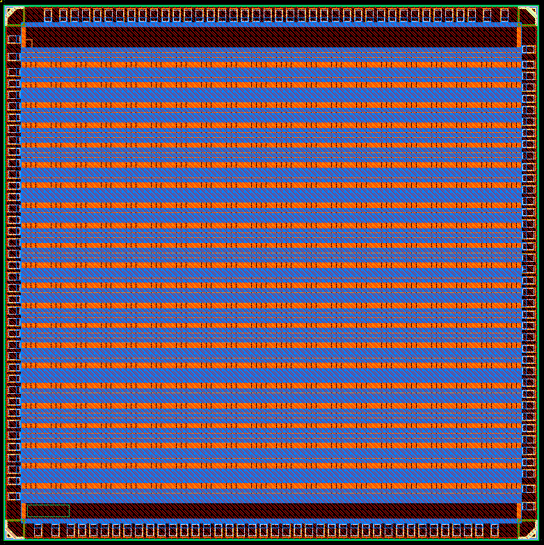
| IP개요 | Our academic research laboratory specializes in designing advanced electronic circuits, spanning a wide range of applications. The proposed project aims to bridge the gap between academic innovation and industrial application by leveraging your chip fabrication expertise to bring our circuit designs to life. Technical Specifications: 1. Low Power Consumption: The PLL chip is engineered to consume less than 500 uW of power, an achievement that surpasses existing benchmarks in scientific literature. This energy-efficient approach aligns with your foundry's commitment to sustainability. 2. Compact Size: The chip occupies a mere 40u by 4u area, a remarkable feat compared to industry standards. This compactness opens doors to applications requiring space-saving solutions. 3. Broad Frequency Range: The PLL chip boasts an impressive operating frequency range, spanning 1GHz to 10GHz. This versatility ensures its utility across a wide range of communication and signal processing systems. In conclusion, we believe that this proposal represents a unique and groundbreaking opportunity. We are excited about the potential impact of our advanced PLL chip and the benefits it can bring to various sectors. We kindly request your support in realizing this project, which has the potential to revolutionize integrated circuit technology. |
||
- 레이아웃 사진 -
|
|||