| IP개요 |
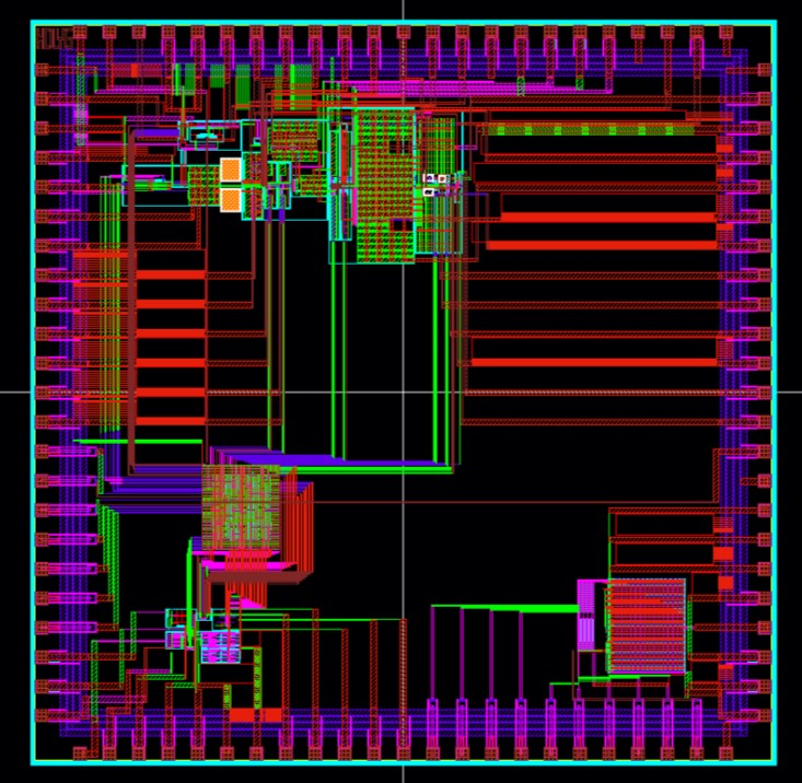
The design circuit will Designing Low Power Transceiver in 180nm CMOS. As the communication method which has low power and excellent processing gain and is designed as a reception structure suitable for IoT. A direct-conversion transceiver that does not use an intermediate frequency is a digital to analog converter (DAC), a variable-gain amplifier (VGA), a low noise amplifier (LNA), and PLL (Phase Locked Loop) blocks. This RF chip is designed for the 180nm process, with a supply voltage of 1.8V and a maximum operating frequency of 915MHz. |