| IP개요 |
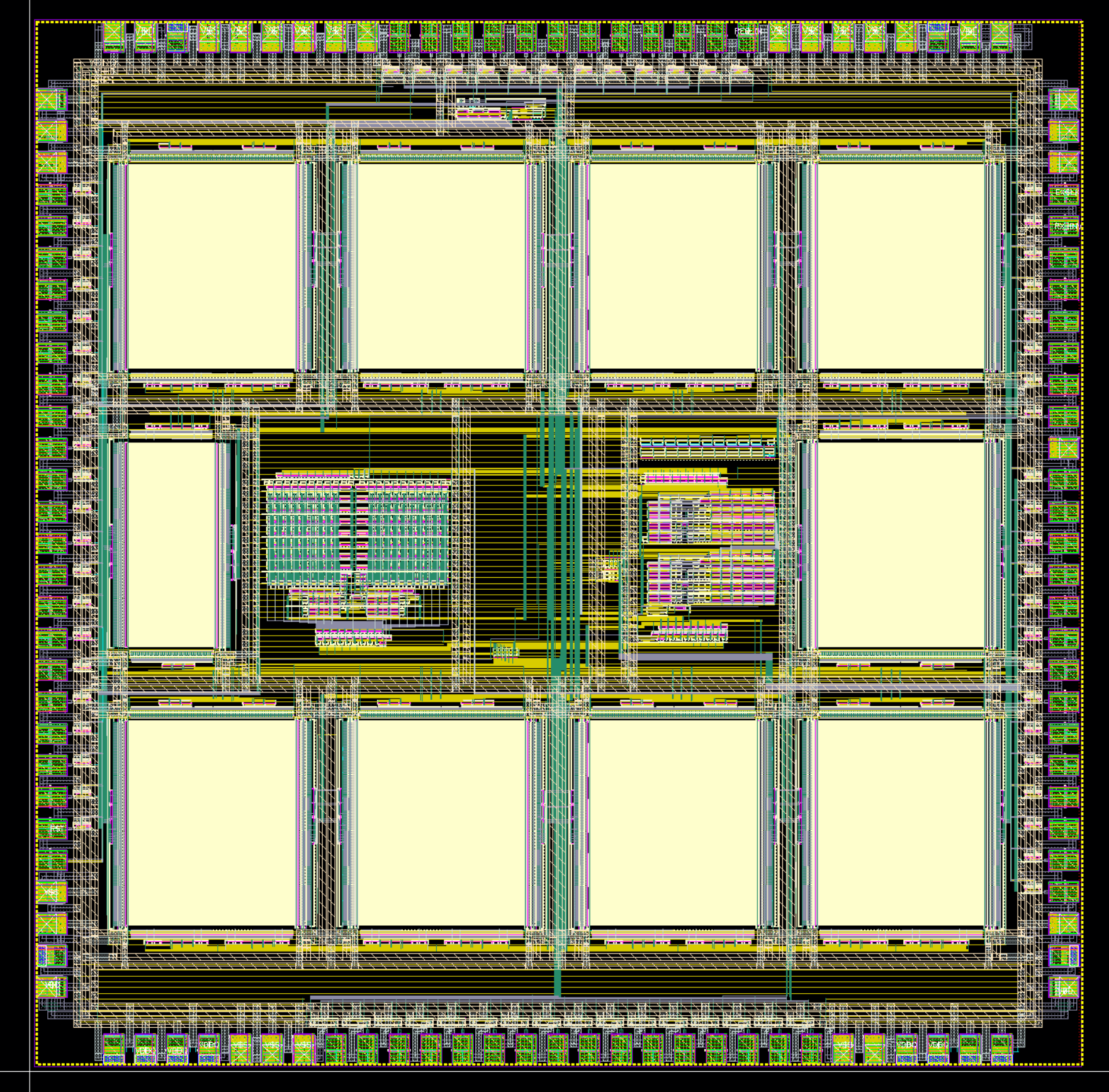
This IP presents a low-power CMOS address-event receiver design that efficiently interfaces event-based vision sensors with neuromorphic processors. The receiver, implemented in 180-nm CMOS technology, features ten groups of 8T SRAM arrays for robust event buffering, with each group containing a 128 × 128 cell array. The design incorporates self-biasing receivers and wake-up circuitry to minimize power consumption, while implementing a four-phase handshaking protocol for reliable asynchronous data reception. The receiver efficiently handles event data from a 128 × 128 pixel vision sensor and converts the asynchronous input to synchronous output for neural network processing. Operating at 1.8V nominal supply voltage, the chip achieves a maximum throughput of 1 million events per second with 4μs latency while consuming only 4mW under typical conditions. The complete system, occupying a 3mm × 3mm die area, demonstrates reliable operation across varying supply voltages (1.6V-2.1V) and temperatures (0°C-85°C), making it particularly suitable for portable and energy-constrained neuromorphic vision applications. |


