


| IP명 | Embedded Flash Memory-Based Compute-in-Memory with Integrated In-Memory Analog-to-Digital Converter | ||
|---|---|---|---|
| Category | Analog | Application | Compute in Memory |
| 실설계면적 | 4㎛ X 4㎛ | 공급 전압 | 10V |
| IP유형 | Hard IP | 동작속도 | DCHz |
| 검증단계 | Silicon | 참여공정 | SS28-2501 |
| IP개요 | We propose a novel ADC architecture that leverages embedded flash (e-flash) memory technology. Our approach integrates an in-memory ADC within a compute-in-memory macro, utilizing both 4T and 2T e-flash cell configurations. Unlike conventional designs that separate program and erase paths via additional transistors, our design employs a unified path, thereby reducing the number of signal lines and transistor count. The e-flash array is configured as a vertically structured AND-type memory, and specialized voltage biasing schemes are implemented to enable selective programming and erasure without forward biasing critical junctions. |
||
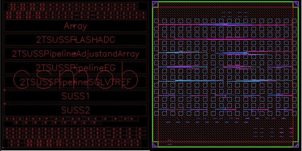
- 레이아웃 사진 -
|
|||