


| IP명 | Design of Low-Phase-Noise Voltage-Controlled Oscillators for Low-Jitter Clock Generation Using Active Source Degeneration and Self-Injection Locking | ||
|---|---|---|---|
| Category | Analog | Application | wireless com. |
| 실설계면적 | 4㎛ X 4㎛ | 공급 전압 | 1V |
| IP유형 | Hard IP | 동작속도 | 20GHz |
| 검증단계 | Silicon | 참여공정 | SF028-2502 |
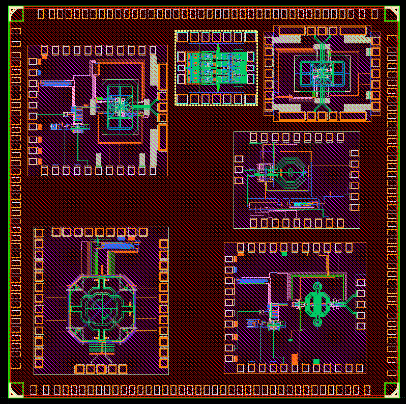
| IP개요 | This work presents three CMOS VCO architectures targeting low-jitter clock generation for wireless communication and high-speed wireline applications. The first design, an active source degeneration dual-core VCO (VCO1), operates over a simulated frequency range of 14.7–16.2 GHz, achieving a 9.7% tuning range with phase noise of –118.6 to –117 dBc/Hz at a 1-MHz offset. The second design, a dual-mode dual-core VCO with active source degeneration and a dual-mode inductor (VCO2), provides frequency reconfigurability across two distinct bands: 15.1–17.2 GHz in mode 1 and 18.1–22.3 GHz in mode 2, with simulated phase noise of 119.7 and –120.2 dBc/Hz at a 1-MHz offset, respectively. The third design, a self-injection-locked VCO with a 2f0 reflector (VCO3), achieves a 20.3% tuning range from 11.5–14.1 GHz and demonstrates a FoM of 186.6 dBc/Hz at 11.9 GHz with a 1-MHz offset and 186 dBc/Hz at a 10-kHz offset. All three VCOs are implemented in a 28-nm FD-SOI CMOS process and validated through post-layout EM simulations. |
||
- 레이아웃 사진 -
|
|||